显示标签为“electronics”的博文。显示所有博文

2015年6月24日星期三

Best Practices in PCB Design: Exporting Gerber Files


Best Practices in PCB Design: Exporting Gerber Files


Overview

This document provides Ultiboard users with practical tips and recommendations on what to do when exporting a PCB design to fabrication.

This document will discuss how to best work with the Ultiboard design environment to generate Gerber files and NC drill files to send to a fabrication house such as Sunstone Circuits.

This is the second in a series of articles that:
  1. Help you finalize for fabrication in Ultiboard
  2. Discuss exporting Gerber files for prototype fabrication
  3. Provide a step-by-step check-list before prototype fabrication

Table of Contents

  1. Creating the Gerber files for PCB Manufacturer
  2. Drill Tables
  3. Next Step

1. Creating the Gerber files for PCB Manufacturer

After verifying all components and completing the final PCB checks, the Gerber files will need to be generated and  uploaded to the board manufacturer’s web page.
For more information on the Gerber Export dialog process, please view this article which provides more context to the dialog box, and what the various settings mean.
Exporting Gerber Files from NI Ultiboard

Gerber Properties

To begin generating the PCB files, the settings for each of the various file types will need to be established.  The first files needed are the Gerber files which allow the manufacturer to create the basic artwork for each of the layers.  From the menu:
  1. Launch the Export setup window from the menu by selecting File > Export….
  2. Ultiboard has default settings for different export schemes such as Fabrication or Fabrication and Assembly
  3. To export Gerbers and Drill files select Fabrication from the drop down menu and the units system used by your board manufacturer
Figure 1 - Export Dialog Box

The RS-274X standard is preferred as it is the most current and widely used Gerber format and automatically assigns the D-code aperture setting whereas the RS-274D requires the manual setup of aperture settings. Aperture D-codes set the basic drawing tool sizes and styles used by the manufacturer to physically create the various layers of the PCB.
In the Gerber properties window, the following Available Layers will be automatically selected, you can add more layers to the export if needed.
  1. Board Outline
  2. All copper layers (Copper Top, Copper Inner 1, Copper Inner 2, Copper Bottom, etc…)
  3. Drill (may be optional for quick turn PCB services using standard drill sizes)
  4. Drill Symbols (may be optional for quick turn PCB services using standard drill sizes)
  5. Silkscreen Top and Silkscreen Bottom (for single sided boards only the top silkscreen layer may be required)
  6. Solder Mask Bottom and Solder Mask Top (may be optional for quick turn PCB services)

It is important to complete the following steps to finalize export: 
  • In the Units section select Imperial (Mil)
  • In the Digits section, select integer 2 and decimal place 4
  • Oversize the Soldermask based on PCB manufacturer’s recommendations (some quick-turn PCB manufactures suggest over sizing the PCB mask to allow for adequate spacing around pads for the solder mask tolerances).
 Now, go the the Output Configuration tab and this where you can define where all the Gerber and Drill files will be saved on your computer. By default it will be set to the same directory where your design file is saved.
Figure 2 - Export Dialog Box Output Configuration


2. Drill Tables

In any PCB, there are typically many holes that need to be drilled for things such as through-hole parts, vias and mounting holes.   There are multiple files relating to the drilling of the holes in the PCB.  The one essential in the creation of the PCB is the NC Drill file (NC = Numerically Controlled).  The NC Drill export selection will create two files, a ‘.drl’ and ‘.rep’. 
The rep is a report file listing a summary of the drill sizes and quantities.  The drill sizes are associated with an individual drill bit (i.e. “tool”) so the tool numbers (“T#”) are shown as each individual sized hole.   If the number of drill sizes can be kept to a minimum, the cost of the PCB will be reduced since it will take less time to switch between sizes when the PCB is being made.
The drl file shows the exact locations of each hole.  It is sorted by the tool number tool number so the PCB manufacturer knows the size and location of all the holes for a specific drill bit size.
In addition, there are two Gerber files that are related to PCB drilling.  The Drill and Drill Symbols are created when the Gerber RS-274Xis selected and subsequently these files are used in documentation such as the assembly drawing to verify all hole sizes and drill locations are correct.
The Drill Gerber file shows round images at each hole with the radius of the image the same as the hole radius.  When viewing this layer, the user can observe the hole sizes, locations and relations to other locations on the PCB.
The Drill Symbols Gerber file has symbols shown for each tool.  For example, if there are 5 different hole sizes needed for drilling into the PCB, there will be 5 different symbols on this Gerber layer.


3. Next Step

Now that you have finalized your design it is time to review the files for fabrications. 
This final article in this series is a prototyping check-list for any engineer looking to use a quick-turn PCB fabrication house, such as PCBWay (www.pcbway.com/e)


website: www.pcbway.com/e


For PCB prototype, please feel easy contact Erin KOU (erin.kou@pcbway.com)

2015年6月10日星期三

PCB share: 20 Tips for Engineering Students

20 Tips for Engineering Students


Getting your engineering degree is a ticket to rewarding careers, and sometimes a handsome paycheck. But before you enter the field as a professional engineer, some serious studying, a few late nights, and a few tips to get you through your first year are in order.

Tip #1: Take good notes, and keep them all after your classes are over.

Engineering textbooks can be dense, but endure through the tedium. Do your reading – all of it – and keep a highlighter and page markers handy. After the class is over, keep your most useful and well-written textbooks as reference. Your notes, annotations, and highlighting will be invaluable later on. You may even want to keep a “Rules of Thumb” notebook, allowing you quick access to your most-used formulas.

Tip #2: Get to know your professors.

Develop a relationship with your professors so you feel comfortable approaching them and asking for help. Get to know one or two key professors particularly well, and turn to them for help with your homework, insight into the industry, and even job or program references.

Tip #3: Ask questions, both in class and out.

Your professors want you to learn. But if the only thing you ever ask is, “Will this be on the test?” then you are not taking advantage of their knowledge or willingness to help. Ask for additional examples to clarify difficult equations and concepts. More often than not, your fellow students will thank you for speaking up, and your professor will appreciate your active investment in the material.

Tip #4: Try to solve a problem before asking for help.

No one wants to do your homework for you. You’ll be more likely to get help if you’ve already begun the effort. Even if you’re totally lost, make a legitimate, prolonged effort to solve a problem before asking for help. When you do seek help, be prepared to discuss what you tried already, and bring your scratch paper showing your attempts.

Tip #5: Form a study group.

Working alone can get exasperating if you find yourself stuck on a problem. Working with others will not only introduce other viewpoints to approaching a problem, it will also provide encouragement and camaraderie in the face of frustration.

Tip #6: Teach someone else.

One of the most effective ways of ensuring you understand something is by explaining it to someone else. Before you move past a subject, make sure you not only answered the question but also can replicate and explain the process. Each new subject and concept will build on the last, so don’t move on until you’ve mastered each new idea.

Tip #7: Diversify your engineering classes.

Take classes in all sorts of engineering, even if they are not your concentration. Understanding not only the subject matter, but also how other types of engineers approach and solve problems, will lend insight into your own field, from biomedical to mechanical to chemical to environmental engineering and beyond.

Tip #8: Take classes outside engineering, particularly design classes.

The most successful engineers are insatiable learners, so seek to broaden your skill set generally. A design class can teach you how to represent information visually and how to talk about an idea from a big picture perspective. A writing class can hone your skills for communicating your ideas to others. A business class can prepare you for organizational tasks and leadership roles later in your career.

Tip #9: Hone your communications skills, including conversation, writing, and presentation.

The best and most innovative ideas in the world have no hope of growing past the drawing board if you are unable to communicate them effectively. And today, most technical communication between team members and leadership happens over email, which is a form of writing. Learn to present an argument simply and without agenda, and always read your emails through once or twice before sending.

Tip #10: Learn another language.

Engineering knows no political or cultural borders; engineers are in demand everywhere in the world. Increase your worth by becoming proficient in another language, and don’t be afraid to think of your career on a global level. Want to build bridges in China? You should learn Mandarin.

Tip #11: Build your portfolio.

Participate in as many hands-on projects as possible, especially those outside the classroom. Future employers look for both coursework and relevant experience, and a well-organized and articulate portfolio will be invaluable during your job search. Your practical project experience will also reinforce the “in theory” knowledge you gain in class.

Tip #12: Get a summer internship.

One of the best portfolio buildings blocks is the summer internship. Internships do more than build your resume; they demonstrate to potential employers that you can commit to a long-term role and work as part of a team.

Tip #13: Build your network.

Do not wait until you need a job to start building professional relationships. In addition to getting to know your professors and peers, attend extracurricular lectures, workshops, and networking events, and get to know as many people working or studying in your field as possible. Take a genuine interest in the work of others, ask lots of questions, and don’t be afraid to seek guidance or advice from those of advanced experience. They were once neophyte engineers too!

Tip #14: Scour the resources of professional engineering associations and companies.

Professional engineering associations, such as the National Society of Professional Engineers, are an invaluable resource for jobs, advice, and networking. Identify organizations that share your values and interests, and make as many contacts as possible.

Tip #15: Skip the honors class.

In the engineering field, your GPA matters. If you struggle in calculus, don’t kill yourself in Honors Calc; take the easier class, learn the material thoroughly, and take the higher grade.

Tip #16: Learn when to lead and when to back down.

Engineers often work in teams, and every team has one or more leaders. You should feel comfortable in both leading and following the directions of others. Hone your leadership skills and learn how to effectively influence group decisions, but recognize when your contribution should be to take orders and follow direction.

Tip #17: Work on the problem before the team meets.

The best results occur when a group discusses ideas that have already been fleshed out by individual members. Learn to do your own work and self-motivate. Always arrive at the team meeting with ideas in mind.

Tip #18: Be a perfectionist.

In the words of one engineer, “In the working engineer world, a 99% correct product can cost millions of dollars in damages.” Adopt the mindset of practicing something until it is perfect, as opposed to going as quickly as possible and settling for a B. When your work is 100%, even if it is slower, it is valuable.

Tip #19: Identify your inspiration.

What made you decide to study engineering? Who do you look up to in your chosen field? Learn about how individuals and companies have sought and found success, and replicate their behaviors.

Tip #20: Take heart and persevere.

Engineering is a difficult course of study for everyone, no matter their IQ or test scores. Frustration can lead to feeling like an imposter. Every future engineer has struggled through seemingly impossible problem sets, cranky professors, and gut-wrenching exams. In the face of inevitable small failures, recognize that you are challenging yourself like never before, and push on through the difficult experiences.


website: www.pcbway.com/e


For PCB prototype, please feel easy contact Erin KOU (erin.kou@pcbway.com)


2015年6月3日星期三

PCB Recycling: The Core of Your Electronics Is More Valuable Than You Think

PCB Recycling: The Core of Your Electronics Is More Valuable Than You Think

By Anne Staley,  Shared by Erin KOU  from PCBWay
The screen you are looking at this very moment will someday be recycled. Electronic recycling is fast becoming just as important as plastic and steel recycling. This is because your household electronic devices – old VCRs, stereo systems, television sets and desktop computers – contain valuable metals and components that can be broken down, recycled and reused. Those dusty shelves in your garage might hold more monetary value than you’re aware of!

What are PCBs?

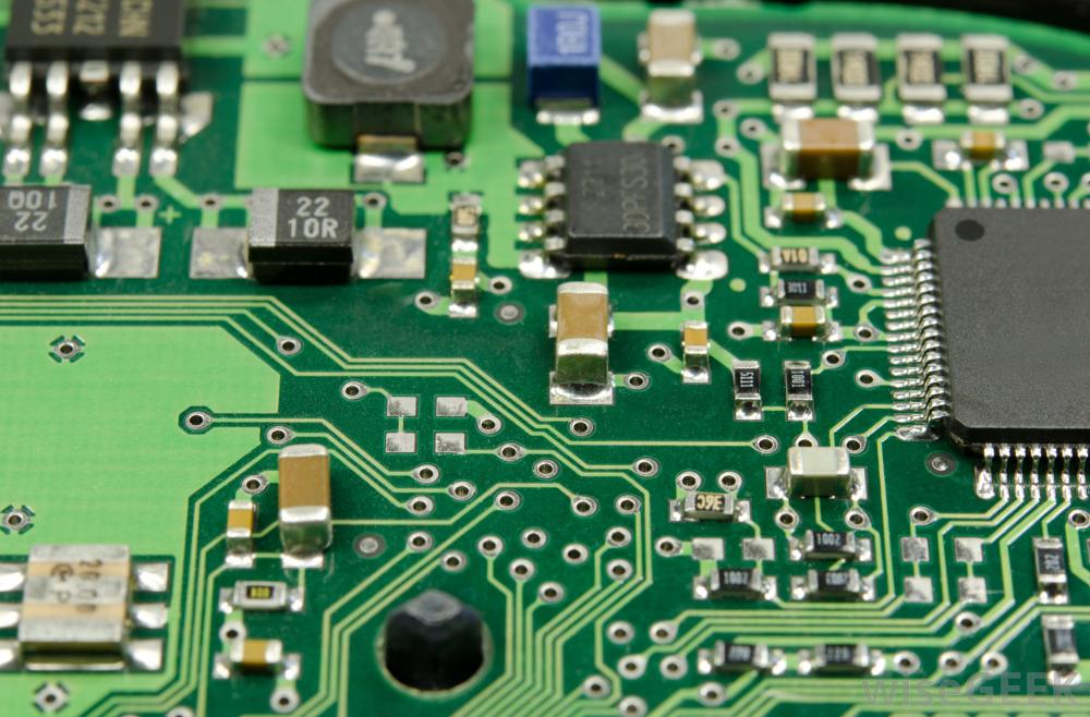
PCBs (or Printed Circuit Boards) are copper-coated plastic layers that connect electrical components using conducting tracks, metals and glass. To the untrained eye, it simply looks like an electronic maze on a green metal plate, but its components are quite special. Electronic waste is made up of PCBs and various cables that require careful demanufacturing by approved recycles so they can be used again.

circuit-board
Source: Wisegeek.org

Why is e-waste valuable?

Computers, microwaves, video cameras – anything that runs on electricity and contains memory chips also contains metals and elements like gold, lead, mercury, iron and cadmium. They also have plastic (the outer casing), glass and fiberglass (the monitor). A major percentage of electronic waste contains plastic, glass and metals, which can (and should) be easily extracted. All of these individual parts can be separated from the unusable elements and refined to manufacture other products.
They are valuable because obtaining these metals means that new metals don’t have to be procured by using raw materials. This e-waste fact sheet suggests that recycling 1 million laptops can save enough energy to power 3,657 U.S. homes for a year.
E-recycling is definitely something that must be practiced by one and all, since it eases the strain put on the earth’s natural resources. Recycling facilities safely remove and dispose of parts that would otherwise rot in landfills and pollute groundwater.

How are electronics recycled?

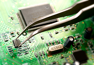
There are two ways in which electronic waste can be recycled–shredding and dismantling. Shredding involves the use of large machine equipment that enables the recovery of recyclable metals from the electronic devices. Dismantling yields more of the smaller components that can easily be put to use again. Taking the electronics apart in this way requires careful manual handling and the use of tools (to remove the smaller ‘bits and pieces’ that make up the electronics we use every day).
Source: Ppa-electronics.com

Some of the PCB components that can be recovered by dismantling are:
  • Capacitors
  • Switches
  • Audio sockets
  • TV plugs
  • Resistors
  • Motor
  • Screws
  • CRTs
  • LEDs
  • Transistors

What can you do?

E-waste/electronic recycling is valuable to the environment, yes, but it can also be valuable to you! Yes, you can sell electronic scrap to waste recycling facilities. Most recycles, like Sims Metal Management, will pay you for your electronic trash. Your EOL (end-of-life) electronics – electronics that have become unusable – can be collected and sold for a good sum to a number of facilities.
 Source: Pacebutler.com          
Source: Pacebutler.com
Some common items that contain PCBs and other recyclable parts are:
  • Laptop and desktop computers
  • Game consoles (Xbox, PlayStation, etc.)
  • Photocopiers
  • Cell phones
  • Video and digital cameras
  • Tablets
  • Speaker systems
  • DVD players
  • GPS devices

The recycling of old electronics is massively helpful to the earth’s resources and the environment. What’s more, it also puts a tidy sum into your pocket. So when the computer you are using right now has reached its EOL, remember that its circuit board, monitor and casing are all valuable and can be traded in at an electronics recycling center.

website: www.pcbway.com/e


For PCB prototype, please feel easy contact Erin KOU (erin.kou@pcbway.com)

2015年5月15日星期五

PCB share: Export Gerber files from Altium


Export Gerber files from Altium

Sourced by Erin KOU [www.pcbway.com/e]

Softwares needed

You need winzip or winrar, you probably already have it installed. If not: winzip or winrar

Export Gerber files from Altium

Design rule check

Make sure you run design rule check (Tools->Design Rule Check...) before you generate Gerber files. DRC usually makes sure that your board doesn’t exceed the manufacturer’s production abilities.
Our PCB manufacturing capabilities are outlined at the home page of http://www.pcbway.com/e, please using Design Rule Wizard to modify the rules accordingly.

Make sure there are no errors. If there are errors, you need to fix them before you can continue to generate Gerber files.

Generate Gerber File

In PCB view, select File -> Fabrication Output -> Gerber files. Then in the popup dialog, select General tab, set Unit to inch and format to 2:5:

General tab

In Layers tab, select "Used On" for the Plot Layers drop down, select "All OFF" for Mirror layers. Check "include unconnected mid-layer pads", and uncheck "Mechanical layers to Add to All plot":
Layers tab

In the Drill Drawing tab, deselect all check boxes, and select Graphic Symbols:
Drill tab

In Apertures tab, make sure RS274X is selected:
Apertures tab

In Advanced tab, select "Separate file per layer" for Batch Mode option. Also select "Suppress leading zeros" for Leading/Trailing Zeros, select "Reference to relative origin" for Position on Film and select "Unsorted" for Plotter Type, then click OK:
Advanced tab

After a few seconds, Gerber files are generated. You don't need to save the generate CAM file, just close it.

Generate NC Drill File

Then in the PCB view, select File -> Fabrication Outputs -> NC Drill Files, in the NC Drill Setup dialog, select "Inches" for Units, "2:5" for Format, "Suppress leading zeros" for Leading/Trailing Zeros and "Reference to relative origin" for Coordinate Positions, then click OK:
NCDrill setup

Click "OK":
Import drill data
Click "OK"
Import mill

Package Gerber File

Altium saves all generated Gerber and NC Drill files in the "Project output folder", usually it is in the same folder as your PCB project folder. Rename the project output folder to something meaningful so you know what it is.
Then zip all files in the output folder and send to us for PCB fabrication.
The following summarizes the Altium Gerber file extensions:
GTL---Top layer
GBL---Bottom layer
GTO---Top overlay
GBO---Bottom overlay
GTP---Top paste
GBP---Bottom paste
GTS---Top solder
GBS---Bottom solder
G1 ---Midlayer 1
G2 ---Midlayer 2
...
GP1---Internal plane 1
GP2---Internal plane 2
...
GM1---Mechanical 1
GM2---Mechanical 2
...
GKO---Keepout layer
GG1---Drill guide
GD1---Drill drawing
GPT---Top pad master
GPB---Bottom pad master
website: www.pcbway.com/e
For PCB prototype, please feel easy contact Erin KOU (erin.kou@pcbway.com)