显示标签为“circuit design”的博文。显示所有博文

2015年6月24日星期三

Best Practices in PCB Design: Exporting Gerber Files


Best Practices in PCB Design: Exporting Gerber Files


Overview

This document provides Ultiboard users with practical tips and recommendations on what to do when exporting a PCB design to fabrication.

This document will discuss how to best work with the Ultiboard design environment to generate Gerber files and NC drill files to send to a fabrication house such as Sunstone Circuits.

This is the second in a series of articles that:
  1. Help you finalize for fabrication in Ultiboard
  2. Discuss exporting Gerber files for prototype fabrication
  3. Provide a step-by-step check-list before prototype fabrication

Table of Contents

  1. Creating the Gerber files for PCB Manufacturer
  2. Drill Tables
  3. Next Step

1. Creating the Gerber files for PCB Manufacturer

After verifying all components and completing the final PCB checks, the Gerber files will need to be generated and  uploaded to the board manufacturer’s web page.
For more information on the Gerber Export dialog process, please view this article which provides more context to the dialog box, and what the various settings mean.
Exporting Gerber Files from NI Ultiboard

Gerber Properties

To begin generating the PCB files, the settings for each of the various file types will need to be established.  The first files needed are the Gerber files which allow the manufacturer to create the basic artwork for each of the layers.  From the menu:
  1. Launch the Export setup window from the menu by selecting File > Export….
  2. Ultiboard has default settings for different export schemes such as Fabrication or Fabrication and Assembly
  3. To export Gerbers and Drill files select Fabrication from the drop down menu and the units system used by your board manufacturer
Figure 1 - Export Dialog Box

The RS-274X standard is preferred as it is the most current and widely used Gerber format and automatically assigns the D-code aperture setting whereas the RS-274D requires the manual setup of aperture settings. Aperture D-codes set the basic drawing tool sizes and styles used by the manufacturer to physically create the various layers of the PCB.
In the Gerber properties window, the following Available Layers will be automatically selected, you can add more layers to the export if needed.
  1. Board Outline
  2. All copper layers (Copper Top, Copper Inner 1, Copper Inner 2, Copper Bottom, etc…)
  3. Drill (may be optional for quick turn PCB services using standard drill sizes)
  4. Drill Symbols (may be optional for quick turn PCB services using standard drill sizes)
  5. Silkscreen Top and Silkscreen Bottom (for single sided boards only the top silkscreen layer may be required)
  6. Solder Mask Bottom and Solder Mask Top (may be optional for quick turn PCB services)

It is important to complete the following steps to finalize export: 
  • In the Units section select Imperial (Mil)
  • In the Digits section, select integer 2 and decimal place 4
  • Oversize the Soldermask based on PCB manufacturer’s recommendations (some quick-turn PCB manufactures suggest over sizing the PCB mask to allow for adequate spacing around pads for the solder mask tolerances).
 Now, go the the Output Configuration tab and this where you can define where all the Gerber and Drill files will be saved on your computer. By default it will be set to the same directory where your design file is saved.
Figure 2 - Export Dialog Box Output Configuration


2. Drill Tables

In any PCB, there are typically many holes that need to be drilled for things such as through-hole parts, vias and mounting holes.   There are multiple files relating to the drilling of the holes in the PCB.  The one essential in the creation of the PCB is the NC Drill file (NC = Numerically Controlled).  The NC Drill export selection will create two files, a ‘.drl’ and ‘.rep’. 
The rep is a report file listing a summary of the drill sizes and quantities.  The drill sizes are associated with an individual drill bit (i.e. “tool”) so the tool numbers (“T#”) are shown as each individual sized hole.   If the number of drill sizes can be kept to a minimum, the cost of the PCB will be reduced since it will take less time to switch between sizes when the PCB is being made.
The drl file shows the exact locations of each hole.  It is sorted by the tool number tool number so the PCB manufacturer knows the size and location of all the holes for a specific drill bit size.
In addition, there are two Gerber files that are related to PCB drilling.  The Drill and Drill Symbols are created when the Gerber RS-274Xis selected and subsequently these files are used in documentation such as the assembly drawing to verify all hole sizes and drill locations are correct.
The Drill Gerber file shows round images at each hole with the radius of the image the same as the hole radius.  When viewing this layer, the user can observe the hole sizes, locations and relations to other locations on the PCB.
The Drill Symbols Gerber file has symbols shown for each tool.  For example, if there are 5 different hole sizes needed for drilling into the PCB, there will be 5 different symbols on this Gerber layer.


3. Next Step

Now that you have finalized your design it is time to review the files for fabrications. 
This final article in this series is a prototyping check-list for any engineer looking to use a quick-turn PCB fabrication house, such as PCBWay (www.pcbway.com/e)


website: www.pcbway.com/e


For PCB prototype, please feel easy contact Erin KOU (erin.kou@pcbway.com)

2015年6月8日星期一

Top 10 PCB Design Software That You Can Use

Top 10 PCB Design Software That You Can Use


By Gulshan jassal  Shared by Erin KOU (PCBWay)

Here is the some of the best PCB design software that can help you to develop your projects. PCB known as the Printed circuit board  that’s are used in the all kinds of the electronics equipments and Gadgets.
The PCB are covered the large technology part for designing the hardware nowdays. There are the various software are used for designing the these boards in order to before they are put in the production.
These software are satisfied different need according to the industry requirement. In this top PCB design software some of the software are industry standards  and beginner level of user (educational use Only) compatible that you can use.

Top 10 PCB Design Software  That You Can Use For Your Different Purpose

  1. bestPCB software
ZinetPCB is the best professional and personal used PCB design software you design free layouts and circuits design.
best free pcb software
This is the Free open source software that run on Windows it is very esay to use and more fast and less complicated
best free pcb software
This program is printer generated output comes under the Mac OS work pretty well on apple Mac OS
best free pcb software
4. TinyCad
This software comes under its own library and very easy to understand layout you can make your free circuits.tinycad-1
This program can used the printer the created the outputs and very user friendly and make your circuits more comparible and good design
best free pcb software
  This software allows the user to produce electronic circuits, while also teaching them more about them
This software allows the user to produce electronic circuits, while also teaching them more about them
This program can be used for the creation of printer circuit boards and electronic schematic diagrams.
8.gEDA
This is a quite popular software that works on Linux. It has been used fr electrical circuit design, prototyping, simulation, schematic capture and production.
This software has been designed to reduce the design to production time. It is one of the most popular electronics design software.
This is a free and open source PCB editor that runs on Windows and was released under the GNU General Public License.

website: www.pcbway.com/e


For PCB prototype, please feel easy contact Erin KOU (erin.kou@pcbway.com)

2015年6月7日星期日

The Engineer’s Guide To High-Quality PCB Design

The Engineer’s Guide To High-Quality PCB Design

Author:  Nicholaus Smith (Application engineer) Sharee by Erin KOU
Eventually, almost every EE must design a PCB, which isn’t something that’s taught in school. Yet engineers, technicians, and even novice PCB designers can create high-quality PCBs for any and every purpose with confidence that the outcome will meet or exceed the objective. Also, these designs can be completed on schedule and within budget while meeting the design requirements. Designers just need to mind the essential documentation, design steps and strategies, and final checks.

Table of Contents

  • The Basic Design Process
  • Bill Of Materials
  • PCB Documentation
  • Schematic Details
  • Component Placement
  • Thermal Issues
  • Fine-Tuning The Component Placement
  • Summary
  • References
The Basic Design Process
The ideal PCB design starts with the discovery that a PCB is needed and continues through the final production boards (Fig. 1). After determining why the PCB is needed, the product’s final concept should be decided. The concept includes the design’s features, the functions the PCB must have and perform, interconnection with other circuits, placement, and the approximate final dimensions.
1. The ideal PCB design flow begins when designers recognize a need that must be fulfilled, and it doesn’t end until testing verifies that the design can meet those needs.

1. The ideal PCB design flow begins when designers recognize a need that must be fulfilled, and it doesn’t end until testing verifies that the design can meet those needs.

Ambient temperature range and concerns regarding the operating environment should be addressed and used to specify the materials selected for the PCB. Components and PCB materials must be selected to guarantee operation under all expected and potential forms of duress the board may be exposed to during its lifetime.
The circuit schematic is drawn based on the concept. This detailed diagram shows the electrical implementation of each function of the PCB. With the schematic drawn, a realistic drawing of the final PCB dimensions should be completed with areas designated for each of the circuit’s schematic blocks (groups of components closely connected for electrical reasons or constraints).
Bill Of Materials
Simultaneously with the schematic’s creation, the bill of materials (BOM) should be generated. The components in the circuit should be selected by analyzing the maximum operating voltages and current levels of each node of the circuit while considering tolerance criteria. With electrically satisfactory components chosen, each component should be reconsidered based on availability, budget, and size.
The BOM must be kept up-to-date with the schematic at all times. The BOM requires the quantity, reference designators, value (numeric value of ohms, farads, etc.), manufacturer part number, and PCB footprint for each component.
These five requirements are critical because they define how many of each part are needed, explain identification and circuit locations while exactly describing each circuit element used for purchasing and substitution, and explain the size of each part for area estimations. Additional descriptions may be added, but it should be a condensed list describing each circuit element, and too much information can over-complicate library development and management.
PCB Documentation
The PCB’s documents should include the hardware dimensional drawings, schematic, BOM, layout file, component placement file, assembly drawings and instructions, and Gerber file set. User guides also are useful but aren’t required. The Gerber file set is PCB jargon for the output files of the layout that are used by PCB manufacturers to create the PCB. A complete set of Gerber files includes output files generated from the board layout file:
  • Silkscreen top and bottom
  • Solder mask top and bottom
  • All metal layers
  • Paste mask top and bottom
  • Component map (X-Y coordinates)
  • Assembly drawing top and bottom
  • Drill file
  • Drill legend
  • FAB outline (dimensions, special features)
  • Netlist file
The special features included in the FAB outline include but are not limited to notches, cutouts, bevels, back-filled vias-in-pad (used for BGA-type IC packages that have an array of pins under the device), blind/buried vias, surface finish and leveling, hole tolerances, layer count, and more.1
Schematic Details
Schematics control the project, so accuracy and completeness are critical for success. They include information that is necessary for the proper operation of the circuit. A schematic should include adequate design details, such as pin numbers, names, component values, and ratings (Fig. 2).
2. Proper schematics, such as this one for the IDTP9021R wireless power receiver’s buck regulator block, include pin numbers, names, component values, ratings, and other vital details.

Consider assembly when designing footprints, and follow the manufacturer’s recommended PCB footprint. Some components come in microscopic packages and do not allow room for extra copper. Even in these cases, a stripe of 2.5 to 3 mils of solder mask should be applied between every pin on the board.Embedded within each schematic symbol is the manufacturer part number used to determine price and specifications. The package specification determines the size of the footprint for each component. The first step should be to make sure the exposed copper for each pin is in the proper location and is slightly larger than the component pins (3 to 20 mils) depending on available area and soldering method.
Follow the rule of 10. Small vias have a finished hole size of 10 mils with 10 additional mils of pad ring. Traces should be 10 mils or further from the edge of the board. Trace-to-trace pitch is 10 mils (5-mil air-gap, 5-mil trace width, 1-oz copper). Vias with 40-mil diameter holes or larger should have a pad ring added for reliability. An additional 15 to 25 mils of clearance beyond the design rule should be instated for copper planes on outer layers from plane to pins. This reduces the risk of solder bridging at all solder points.
Component Placement
Component placement is next in the process and determined based on thermal management, function, and electrical noise considerations. A first-pass component placement step commences after the outline of component and interconnect position has been assigned. Immediately after the individual components are placed, a placement review should be held and adjustments made to facilitate routing and optimize performance.
Placement and package sizes are often reconsidered and changes are made at this point based on size and cost. Components absorbing greater than 10 mW or conducting more than 10 mA should be considered powerful enough for additional thermal and electrical considerations. Sensitive signals should be shielded from noise sources with planes and be kept impedance-controlled.  
Power management components should utilize ground planes or power planes for heat flow. Make high-current connections according to the acceptable voltage drop for the connection. Layer transitions for high current paths should be made with two to four vias at each layer transition.Place multiple vias at layer transitions to increase reliability, reduce resistive and inductive losses, and improve thermal conductivity.
Thermal Issues
The heat generated by the IC is transferred from the device to the copper layers of the PCB (Fig. 3). The ideal thermal design will result in the entire board being the same temperature. The copper thickness, number of layers, continuity of thermal paths, and board area will have a direct impact on the operating temperature of components.
3. IC thermal conduction can be achieved through the use of thermal vias and copper planes.

To reduce operating temperatures easily, use more layers of solid ground or power planes connected directly to heat sources with multiple vias. Establishing effective heat and high-current routes will optimize heat transfer by means of convection. The use of thermally conductive planes to spread the heat evenly dramatically lowers the temperature by maximizing the area used for heat transfer to the atmosphere (Fig. 4).2
4. Effective heat spreading can distribute the heat uniformly from a heat source to all of the PCB’s exposed surfaces.

With even heat distribution, the following formula can be used to estimate surface temperatures:
P = (heatConvection) x area x (ΔT)     
where:
P = power dissipated on the board
Area = board (X axis x Y axis)
ΔT = surface temperature – ambient temperature
HeatConvection = convection constant based on ambient conditions
Fine-Tuning The Component Placement
Components should be placed in the following order: connectors, power circuits, sensitive and precision circuits, critical circuit components, and then the rest. The schematic is built around each part on the PCB and completely interconnected. Routing priority for the circuit is chosen based on power levels, noise susceptibility, or generation and routing capability.
In general, trace widths of 10 to 20 mils are used for traces carrying 10 to 20 mA and 5 to 8 mils for traces carrying less current than 10 mA. High-frequency (greater than 3 MHz) and rapidly changing signals should be carefully considered when routed along with high-impedance nodes.
The lead engineer/designer should review the layout, and physical locations and routing paths should be adjusted iteratively until the circuit is optimized for all design constraints. The number of layers depends on power levels and complexity. Add layers in pairs since the copper cladding is produced that way. The routing of power signals and planes, the grounding scheme, and the board’s ability to be used as intended all influence operation.
Final inspections should involve verification that sensitive nodes and circuits are properly shielded from noise sources, solder mask exists between pins and vias, and the silkscreen is clear and concise. When determining layer stack-up, use the first inner layer below the component sides as ground and assign power planes to other layers. Stack-ups are created in a manner that balances the board relative to the midpoint of the Z axis.
Consider any concerns the PCB designer has during the reviews, and correct the PCB based on feedback generated by the reviews. Create and verify lists of changes during each review iteration until the board is finalized. During all stages of the layout, keep the design error free by using the design rule checker (DRC).
The DRC can only catch errors that it has been programmed to monitor, and DRC rule sets often change based on individual designs. At the minimum, the design rule checking should cover package-to-package spacing, unconnected nets (a unique name identifying each node of the circuit), shorted nets, air-gap violations, if vias are too close to solder pads, if vias are too close to each other, and vertical clearance violations.
Many other important DRC rules can be set to ensure a robust design, and they should be researched and understood. For example, keep clearances at or above 5 mils. Vias should not be located within surface-mount pads (unless back-filled). And, solder mask should be between all solder points.
Cost is often a driving influence behind PCB design, so it is good to understand the cost adders in PCB manufacturing. A typical board is two to four layers, with no drill holes less than 10 mils in diameter and 5-mil minimum air gaps and trace widths. It also should be 0.062 in. thick with standard FR-4 and a copper foil weight of 1 oz. Additional layers, extra thick or thin boards, vias-in-pad, back-filled vias (non-conductive preferred due to conductivity limitations and thermal expansion differences), blind/buried vias, and lead time all substantially add to the overall cost.
Manufacturer capabilities should be understood when the PCB design commences. PCB fabs are routinely contacted about capabilities and cost reduction techniques when designing PCBs for manufacturability.
Summary
PCB design may be complex, but it is quite possible to design good boards with a little technique and practice. Using these guidelines and adding research when needed, seasoned veterans may continue honing their skills and novice designers may learn to create high-quality PCBs that exceed expectations.
References
1. Cohen, Patricio, Concepts and terminology used in Printed Circuit Boards (PCB), Electrosoft Engineering, Web, May 25, 2013.
2. Mauney, Charles, Thermal Considerations for Surface Mount Layouts, Texas Instruments, Web, May 13, 2013.

website: www.pcbway.com/e


For PCB prototype, please feel easy contact Erin KOU (erin.kou@pcbway.com)

PCB Design Tips | General Electronics Tutorial


PCB Design Tips | General Electronics Tutorial


website: www.pcbway.com/e


For PCB prototype, please feel easy contact Erin KOU (erin.kou@pcbway.com)

2015年6月3日星期三

PCB Recycling: The Core of Your Electronics Is More Valuable Than You Think

PCB Recycling: The Core of Your Electronics Is More Valuable Than You Think

By Anne Staley,  Shared by Erin KOU  from PCBWay
The screen you are looking at this very moment will someday be recycled. Electronic recycling is fast becoming just as important as plastic and steel recycling. This is because your household electronic devices – old VCRs, stereo systems, television sets and desktop computers – contain valuable metals and components that can be broken down, recycled and reused. Those dusty shelves in your garage might hold more monetary value than you’re aware of!

What are PCBs?

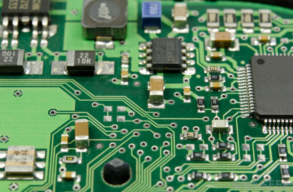
PCBs (or Printed Circuit Boards) are copper-coated plastic layers that connect electrical components using conducting tracks, metals and glass. To the untrained eye, it simply looks like an electronic maze on a green metal plate, but its components are quite special. Electronic waste is made up of PCBs and various cables that require careful demanufacturing by approved recycles so they can be used again.

circuit-board
Source: Wisegeek.org

Why is e-waste valuable?

Computers, microwaves, video cameras – anything that runs on electricity and contains memory chips also contains metals and elements like gold, lead, mercury, iron and cadmium. They also have plastic (the outer casing), glass and fiberglass (the monitor). A major percentage of electronic waste contains plastic, glass and metals, which can (and should) be easily extracted. All of these individual parts can be separated from the unusable elements and refined to manufacture other products.
They are valuable because obtaining these metals means that new metals don’t have to be procured by using raw materials. This e-waste fact sheet suggests that recycling 1 million laptops can save enough energy to power 3,657 U.S. homes for a year.
E-recycling is definitely something that must be practiced by one and all, since it eases the strain put on the earth’s natural resources. Recycling facilities safely remove and dispose of parts that would otherwise rot in landfills and pollute groundwater.

How are electronics recycled?

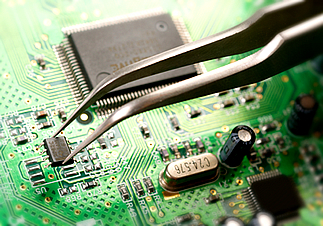
There are two ways in which electronic waste can be recycled–shredding and dismantling. Shredding involves the use of large machine equipment that enables the recovery of recyclable metals from the electronic devices. Dismantling yields more of the smaller components that can easily be put to use again. Taking the electronics apart in this way requires careful manual handling and the use of tools (to remove the smaller ‘bits and pieces’ that make up the electronics we use every day).
Source: Ppa-electronics.com

Some of the PCB components that can be recovered by dismantling are:
  • Capacitors
  • Switches
  • Audio sockets
  • TV plugs
  • Resistors
  • Motor
  • Screws
  • CRTs
  • LEDs
  • Transistors

What can you do?

E-waste/electronic recycling is valuable to the environment, yes, but it can also be valuable to you! Yes, you can sell electronic scrap to waste recycling facilities. Most recycles, like Sims Metal Management, will pay you for your electronic trash. Your EOL (end-of-life) electronics – electronics that have become unusable – can be collected and sold for a good sum to a number of facilities.
 Source: Pacebutler.com          
Source: Pacebutler.com
Some common items that contain PCBs and other recyclable parts are:
  • Laptop and desktop computers
  • Game consoles (Xbox, PlayStation, etc.)
  • Photocopiers
  • Cell phones
  • Video and digital cameras
  • Tablets
  • Speaker systems
  • DVD players
  • GPS devices

The recycling of old electronics is massively helpful to the earth’s resources and the environment. What’s more, it also puts a tidy sum into your pocket. So when the computer you are using right now has reached its EOL, remember that its circuit board, monitor and casing are all valuable and can be traded in at an electronics recycling center.

website: www.pcbway.com/e


For PCB prototype, please feel easy contact Erin KOU (erin.kou@pcbway.com)